Renesas PK-S5D9
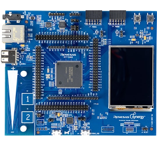
The PK-S5D9 is a single-board kit for the Renesas Synergy S5D9 Group Microcontrollers (MCUs), with a 176-pin LQFP package. The board provides easy-to-access interfaces to the peripherals of the S5D9 Group MCUs for application development. The PK-S5D9 includes four header connectors for direct access to the I/O pins in the MCU, and connectors for USB, Ethernet, RS-232/485, and CAN. The PK-S5D9 incorporates a 2.4-in. QVGA (240 x 320) TFT display with capacitive touch screen.As a promotion kit, the PK-S5D9 is designed to demonstrate the main features of the Synergy Platform using the S5D9 Group MCUs. This is an initial evaluation platform that you can use to determine which kit is appropriate for further development of your product.
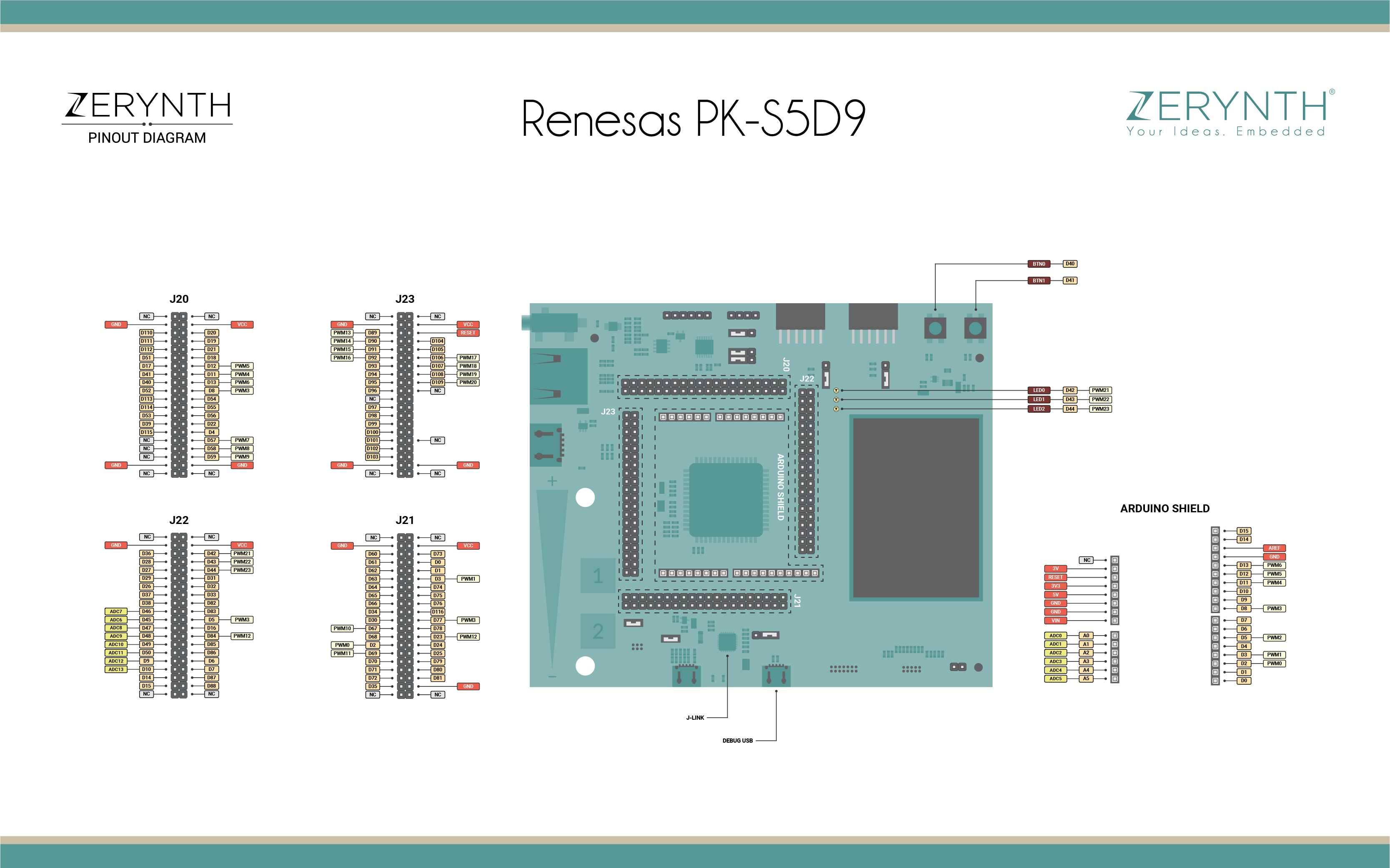
Pin Mapping
Renesas PK-S5D9 official manual is available here
Flash Layout
The internal flash of the Renesas PK-S5D9 is organized into one bank of 2Mb with 70 total sectors of different size according to the following table:
| Start address | Size | Content |
|---|---|---|
| 0x00000000 | 8Kb | Reserved |
| 0x00002000 | 8Kb | Reserved |
| 0x00004000 | 8Kb | Reserved |
| 0x00006000 | 8Kb | Reserved |
| 0x00008000 | 8Kb | Reserved |
| 0x0000a000 | 8Kb | Reserved |
| 0x0000c000 | 8Kb | Reserved |
| 0x0000e000 | 8Kb | Reserved |
| 0x00010000 | 32Kb | Reserved |
| 0x00018000 | 32Kb | Reserved |
| 0x00020000 | 32Kb | Virtual Machine |
| 0x00028000 | 32Kb | Bytecode Slot 0 |
| 0x00030000 | 32Kb | Bytecode Slot 1 |
| 0x00038000 | 32Kb | Bytecode Slot 2 |
| ... | ... | ... |
| 0x001F8000 | 32Kb | Bytecode Slot 59 |
Device Summary
- Microcontroller: ARM 32-bit Cortex™-M4 CPU Core
- Operating Voltage: 3.3V
- Input Voltage: 5V
- Digital I/O Pins (DIO): 116
- Analog Input Pins (ADC): 13
- SPIs: 3
- I2Cs: 1
- Flash Memory: 2Mb
- SRAM: 640 Kb
- Clock Speed: 120MHz
Power
Power is supplied to the PK-S5D9 through the debug USB connector (J19). The PK-S5D9 requires 5V applied on this interface (USB standard). Once power is supplied, the power supply indicator lights up in green.
The MCU digital power supply power consumption can be measured by removing the J31 jumper and measuring the current draw across it. Power consumption for the MCU analog supply requires removing resistor R114 and measuring current across it.
Connect, Register, Virtualize and Program
The Renesas PK-S5D9 needs an FTDI USB to Serial converter connected to the SERIAL0 (on the Arduino Shield) to be programmed.
Once both the FTDI and the Debug Port are connected on USB ports, the PK-S5D9 is recognized by Zerynth Studio and listed in the Device Management Toolbar. The next steps are:
- Select the Renesas PK-S5D9 on the Device Management Toolbar (disambiguate if necessary);
- Register the device by clicking the “Z” button from the Zerynth Studio;
- Create a Virtual Machine for the device by clicking the “Z” button for the second time;
- Virtualize the device by clicking the “Z” button for the third time.
Note
No user intervention on the device is required for registration and virtualization process.
After virtualization, the PK-S5D9 device is ready to be programmed and the Zerynth scripts uploaded. Just Select the virtualized device from the “Device Management Toolbar” and click the dedicated “upload” button of Zerynth Studio.
Important
A microcnotroller serial port (UART) is not available over the ST-Link interface (mini USB - J19); to visualize serial messages or debug messages over the Zerynth console and to program the device a second USB cable must be connected to the SERIAL0 by the use of an FTDI USB to Serial.
Missing features
Not all features have been included in the Renesas PK-S5D9 VMs. In particular the following are missing but will be added in the near future:
- CDC Driver to program the board without an FTDI device
- LCD Screen Drivers
- Ethernet Driver
- CAN
- Capacitive Touch Interface driver
- Audio Output